Hacking a 2014 tablet... in 2024!
Posted on Sun 21 July 2024 in writeup
Yes, you heard that right, 10 years after its release, I managed to hack and unlock the first MediaTek based Amazon tablet that went on sale, the Amazon Fire HD6 / HD7 2014 (codenamed ariel).
In this article, I'll explain my journey in detail without making it too long. If you prefer to skip ahead and see the source code directly (no judgment, I don't like to read or write much either :P), you can find it here!
Introduction
You might be wondering why I decided to tinker with such an old device, especially after so much time has passed since its release. The reason is simple: its SoC. While MediaTek devices are quite common, this tablet features a unique SoC, the MT8135.
So, what’s so special about it? Well, nothing much, really. It feels like a tablet version of the MT6595, which was used in phones like the Meizu MX4. The real interest lies in the fact that no one has managed to unlock this device due to its unique quirks which we'll see as soon as the article develops.
Getting the device
Although it may sound stupid, the first problem I encountered was finding the device, as it was never sold in Spain. In total, throughout my journey, I acquired two HD7s and two HD6s (one of which eventually died).
The first unit was purchased from Wallapop, a popular platform for buying and selling second-hand products in Spain. The two HD7s were bought from eBay and imported directly from the U.S., which cost me quite a bit. The former HD6 was generously donated by kip_dynamite, to whom I owe a huge thanks.
Analyzing the firmware
As seen on other Amazon devices, this tablet runs a heavily modified version of Android called FireOS. To my surprise, it was released with FireOS 4 (based on Android 4) but received an update to FireOS 5 (based on Android 5.1.1).
Given that this is such an old device, I assumed its firmware would be similar to the 2015 Fire 7. So, I proceeded to download the latest stock firmware available for this device and extracted it. The result surprised me because something very important seemed to be missing... or at least that was my initial impression.
r0rt1z2@r0rt1z2-pc:~/Downloads/update$ tree -L 2
.
├── boot.img
├── file_contexts
├── images
│   ├── lk.bin
│   └── tz.img
├── META-INF
│   ├── CERT.RSA
│   ├── CERT.SF
│   ├── com
│   └── MANIFEST.MF
├── ota.prop
├── system
│   └── build.prop
├── system.new.dat
├── system.patch.dat
└── system.transfer.list

5 directories, 12 files
r0rt1z2@r0rt1z2-pc:~/Downloads/update$
In case you haven't noticed, the Preloader image is missing. As I mentioned before, this device has quite a few special quirks, and this is one of them.
After realizing the Preloader was missing, I decided to do some research and came across an XDA thread that provided the location of TX and included a few UART logs from an HD6. Fortunately, one of the log links was still working, allowing me to understand how the boot chain worked on this device.
[PL0] Build Time: 20140829-000812
...
That is the very first line of the log. It looks like the PreLoader printing its build time, but what does that 0 stand for? If we read a few more lines, we can find the answer to that question:
[PL0] loading partition 'TEE1' offset=00300000 at address=12001000
...
[PART] load "2" from 0x0000000001800200 (dev) to 0x12001000 (mem) [SUCCESS]
[PART] load speed: 9999KB/s, 112636 bytes, 11ms
...
[PL0]image verification passed for PL1[key0]
[PL0] PL1 Load OK from TEE1: err=0
[PL0] jump to 12001000
Apparently, Preloader is divided into two different stages:
-
PL0: This stage initializes the eMMC, sets up the clock and bus width, and parses the GPT to identify partitions. It then loads and verifiesPL1from theTEE1partition before jumping to execute it. -
PL1: This stage initializes the PMIC, I2C, performs hardware checks, sets up the RTC, DRAM, and initializes the boot device. It then verifies and loadsLKandTEEimages, performs cryptographic checks, and sets up the boot arguments. Finally, it jumps to theTEEimage to continue the boot process.
With this information, I extracted the latest PL1 image from the tz.img we previously downloaded. Knowing its offset is 0x00300000 (as seen in the UART log), I used UNIX dd to cut the image:
r0rt1z2@r0rt1z2-pc:~/Downloads/update/images$ dd if=tz.img of=PL1.img bs=1 skip=$((0x00300000))
113328+0 records in
113328+0 records out
113328 bytes (113 kB, 111 KiB) copied, 0.234714 s, 483 kB/s
r0rt1z2@r0rt1z2-pc:~/Downloads/update/images$ hexdump -C PL1.img | head -n5
00000000  88 16 88 58 b0 b8 01 00  50 4c 31 00 00 00 00 00  |...X....PL1.....|
00000010  00 00 00 00 00 00 00 00  00 00 00 00 00 00 00 00  |................|
00000020  00 00 00 00 00 00 00 00  ff ff ff ff ff ff ff ff  |................|
00000030  ff ff ff ff ff ff ff ff  ff ff ff ff ff ff ff ff  |................|
*
r0rt1z2@r0rt1z2-pc:~/Downloads/update/images$
Success! We've obtained a clean dump of the second Preloader stage image. Regarding the other parts of firmware, everything was similar, if not identical, to the Fire 7 2015. Both LK and the rest of the TZ function the same way, and FireOS has the same structure. For those interested, I have uploaded a full dump on my dumpyard.
Rooting the device
To play it safe, I thought it would be best to root the device. Before acquiring it, I read XDA and informed myself about the available options.
The latest versions of FireOS 5 are not rootable, but it's always possible to downgrade (without bricking) to FireOS 4.5.3 and root from there using KingoRoot (yes, I also hate these one-click root solutions too; they are the worst).
The problem with this method is that KingoRoot requires an internet connection. If you connect to some Wi-Fi while on 4.5.3, Amazon will automatically (and instantly) download a software update and subsequently install it, causing a hard brick on the device (I'm speaking from experience :D).
To avoid this, I decided to sniff out and extract whatever KingoRoot's black magic is, and put everything together into a ZIP file to create a safe offline rooting method. This method directly installs SuperSU instead of the usual Chinese bloatware! I won't go into details here, but if you want to see how it works, check out this XDA thread.
shell@ariel:/data/local/tmp $ su
root@ariel:/data/local/tmp # id
uid=0(root) gid=0(root) context=u:r:init:s0
root@ariel:/data/local/tmp #
(g0t r00t!)
Accessing UART
As I mentioned earlier, an XDA user had posted the TX location on the HD6 board a few years ago, which made my life easier.
I decided to open up my HD7 to try to solder the TX connection, allowing me to more easily debug amonet, as UART is usually necessary for this process. I opened the back of the device and the first thing I found was a completely different PCB layout, which scared the hell out of me. Did this mean that finding the TX would not be as easy as I had hoped?
Thankfully, my fears were unfounded. In the picture posted by the XDA user, you could see that the TX was part of what looked like a JTAG test point labeled JDEBUG1. After a quick inspection of my HD7 board, I noticed the same label was present so my partner helped me to solder the pin in the same position as shown in the XDA image.
To be able to close the back of the tablet, we made a hole in the right side of the chassis and carefully passed both cables through it. The result was pretty solid, and it still holds up just fine as I'm writing this article!
I plugged in the device and... voila! UART was working just fine, I was able to read the output of PL0, PL1 and the rest of bootloader images:
[21:50:51.343] Warning: Could not open tty device (No such file or directory)
[21:50:51.343] Waiting for tty device..
[21:50:56.839] Connected to /dev/ttyUSB0

[PL0] Build Time: 20140925-030705
[SD0] Bus Width: 1
...
Accessing bootROM mode
Typically, on such devices, we'd use the first stage of amonet, which exploits a vulnerability in bootROM to upload and execute custom payloads. However, to do this, we'd need to access USDBL mode first, which is something nobody has been able to achieve on this particular device.
Volume keys
I decided to run strings on the previously extracted PL1 image to check for any references to USBDL mode, and I found the following:
r0rt1z2@r0rt1z2-pc:~/Downloads/update/images$ strings PL1.img | grep -e "emergency" -e "download"
...
%s exit emergency dl mode due to time-out (%d ms, %d ms)
download keys are pressed
[RTC] clear emergency dl mode flag in rtc register
[RTC] emergency dl mode flag in rtc register is detected
%s emergency download mode(timeout: %ds).
[RTC] use pl dl mode for emergency dl mode
r0rt1z2@r0rt1z2-pc:~/Downloads/update/images$
Technically, if the image wasn't lying, this mode should be accessible through the volume rocker, similar to the first versions of the Fire 7 2015's Preloader. So, I decided to give it a try:
r0rt1z2@r0rt1z2-pc:~$ lsusb | grep MT
Bus 003 Device 007: ID 0e8d:3000 MediaTek Inc. MT65xx Preloader
r0rt1z2@r0rt1z2-pc:~$ lsusb
After a few tries, I concluded no MT6627 (which is what bootrom identifies with) showed up at all, so this probably got patched by Amazon :(
Erasing Preloader from the eMMC
The next thing I tried was quite risky, but as we say in Spanish, "quien tenga miedo a morir, que no nazca" (those who fear death should not be born). It involves erasing /dev/block/mmcblk0boot0 so that bootROM fails to load the Preloader and falls back to USBDL mode:
root@ariel:/ $ echo 0 > /sys/block/mmcblk0boot0/force_ro
root@ariel:/ $ dd if=/dev/zero of=/dev/block/mmcblk0boot0 bs=512 count=8
8+0 records in
8+0 records out
4096 bytes transferred in 0.001 secs (4096000 bytes/sec)
root@ariel:/ $ echo -n EMMC_BOOT > /dev/block/mmcblk0boot0
root@ariel:/ $ reboot -p
... and it booted back to the OS, as if nothing happened! I double checked mmcblk0boot and it remained intact so... what's exactly going on here?
After hours of research, I discovered that the persisbackup partition seemed to contain factory logs from when the device was first programmed and this is what I found:
Boot Area Write protection [BOOT_WP]: 0x04
  Power ro locking: possible
  Permanent ro locking: possible
  partition 0 ro lock status: locked permanently
  partition 1 ro lock status: not locked
Looks like Amazon locked down the first stage of Preloader on purpose... but why? That's something I discovered after hard bricking my Fire HD6.
Shorting the eMMC
I really didn't want to go to this extreme, as I only had my first HD6 at the time, but I decided to be brave and disassemble the device. Considering this method is meant to work in 100% of cases unless USBDL mode was disabled, I wondered: this is a 2014 device—did Amazon really disable it, like on newer models?
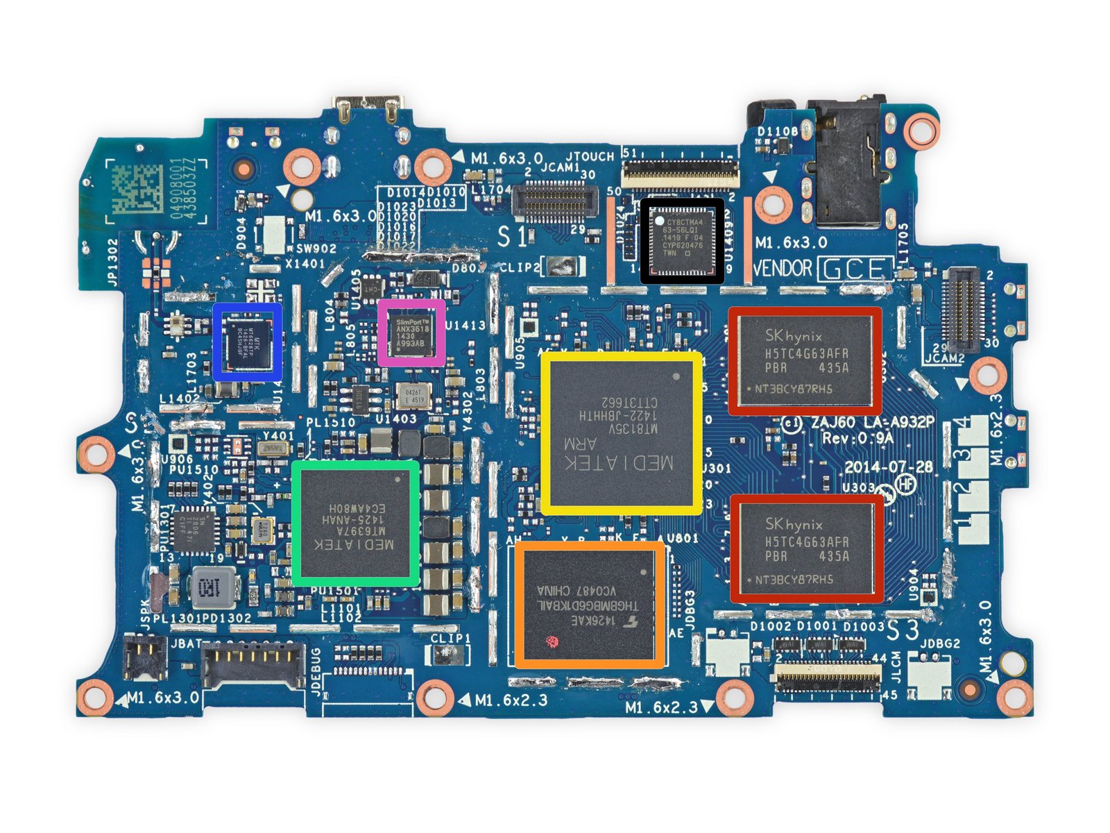
As seen in the picture (courtesy of iFixit), everything is protected (or covered) by a soldered metal shield, so I had to use my soldering iron. Since I'm not very skilled at soldering, I asked my partner, who has excellent soldering skills, to help me with this.
The result was fairly good, except for the fact that we accidentally ripped off what seemed to be a capacitor related to the screen.
After that, I started playing the lottery (a very bad mistake—DON'T ever try this at home) with what I thought could be CLK, CMD, or even DAT0. Unfortunately, after a few shorts, I ended up killing the device to the point where it wouldn't even try to boot. So, there goes my first unit :D
UART. What's going on?
Since we had already found TX (which is enough to read UART logs), I decided to see what was happening when trying to access USBDL mode, either by shorting or using the volume rocker. Here's what I discovered:
key 1 is pressed
[LIB] invalid susbdl config '0xEA000007'
<ASSERT> seclib_dl.c:line 62 0
[PLFM] preloader fatal error...
That's what happens when you press the volume down key while connecting the device to the PC. Apparently, the Preloader detects the key press and triggers an assert, which should cause a reboot to bootROM mode. Unfortunately, in my case, it rebooted normally :(
Exploiting the Preloader
Having concluded that USBDL mode was not accessible, I decided to focus on exploiting the Preloader to gain arbitrary code execution and subsequently upload my own payloads.
Since we know that both the Preloader and bootROM support the same commands, I decided to use the same method as the one employed for the Fire HD8 2018, which exploited the GCPU to read and write memory addresses arbitrarily.
My initial goal was to dump the bootROM, but as you'll see later, I failed miserably. However, I did manage to achieve code execution in the Preloader, which is a significant result nonetheless. :)
What's bootROM?
After the CPU initializes, the internal SRAM controller pushes a jump instruction to the bootROM address. This is the first code that runs on the device, and it can't be modified. The bootROM takes care of initializing basic hardware such as flash storage, UART1 (the first serial port), loading the Preloader into the On-Chip SRAM, and jumping to it.
While bootROM is usually located at 0x0, there are certain cases where that address contains a direct jump to either 0x00400000 or 0x48000000, as seen in bypass_payloads.
r0rt1z2@r0rt1z2-pc:~ $ hexdump -C 6572_0x0.bin | head -n 1
00000000  04 f0 1f e5 00 00 40 00  00 00 00 00 00 00 00 00  |......@.........|
r0rt1z2@r0rt1z2-pc:~ $
As seen above, the MT6572 contains the instruction 04 f0 1f e5, which translates (HEX -> ARM) to LDR pc, [pc, #-4]. This instruction loads the value from address 0x4 into the program counter (PC). Since this value is 0x00400000, the instruction effectively redirects execution to the actual bootROM code.
Dumping bootROM is no easy task, as it requires you to do so within a privileged context. To understand what I mean, let's take a look at the ARM developer documentation:
In the ARMv7 architecture, the processor mode can change under privileged software control or automatically when taking an exception. When an exception occurs, the core saves the current execution state and the return address, enters the required mode, and possibly disables hardware interrupts.
Applications operate at the lowest level of privilege, PL0, previously unprivileged mode. Operating systems run at PL1, and the Hypervisor in a system with the Virtualization extensions at PL2. The Secure monitor, which acts as a gateway for moving between the Secure and Non-secure (Normal) worlds, also operates at PL1.
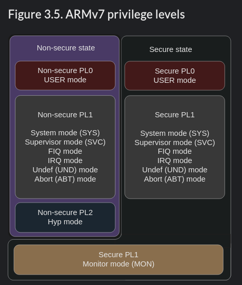
To make things easier to understand, let's just say that on the MT8135, which is ARMv7-based, both the Preloader and the TEE run at the most privileged state. Meanwhile, the Little Kernel (second bootloader) and the kernel operate at a lower privilege level.
Understanding the GCPU exploit
The GCPU is a SoC peripheral designed for decrypting encrypted media, featuring a microcontroller core (Control CPU or CCPU) equipped with ROM, SRAM, and hardware accelerators for various cryptographic algorithms including AES, SHA, MD5, RC4, DES, CRC32, and DMA.
The Control CPU (its microcontroller core) operates with a 22-bit instruction set and includes 32 general-purpose 32-bit registers, instruction ROM, instruction RAM, and data RAM.
Direct interaction with the GCPU is achieved by writing to its memory-mapped registers within the SoC's address space. During the boot process, at least on Amazon devices, both the Preloader and the LK (bootloader) use the GCPU to verify the integrity of the images before loading them into memory. As usual, further reverse engineering of this process can provide deeper insights into the GCPU's functionality :)
In my first attempts to dump bootROM, I didn't have arbitrary code execution capabilities in the LK. Thus, my access to the GCPU was solely through the Preloader.
For my device, an older Preloader version exposed two commands to read and write memory addresses within a predefined range; CMD_READ32 and CMD_WRITE32
As seen in the amonet source code, these can be used to read from and write to the GCPU's registers, and thus trigger cryptographic operations.
To grasp how bootROM data was successfully dumped back then, we need to delve into the intricacies of AES-CBC (Cipher Block Chaining) mode utilized during the decryption processes.
Reading data
AES-CBC mode is a common encryption technique where data is encrypted block by block. Each block of data is XORed with the ciphertext of the previous block before it is encrypted.
During decryption, each block of ciphertext is decrypted and then XORed with the previous block's ciphertext to reconstruct the plaintext. The very first block, however, uses an Initialization Vector (IV) in place of previous ciphertext, setting the stage for the encryption or decryption sequence.
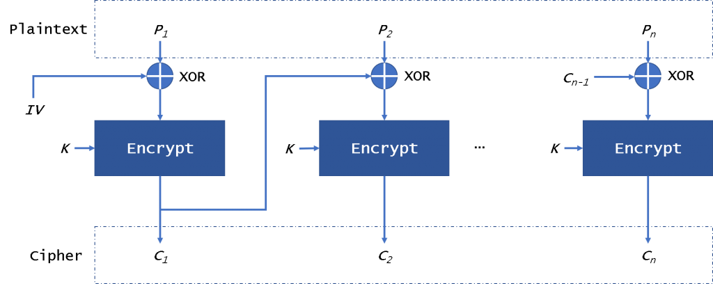
In this scenario, the attacker sets the IV to zero. This is basically done so when the first block is decrypted, the absence of a previous ciphertext block means the plaintext is directly revealed and gets decrypted without any alterations, making it plainly visible.
For example, let's consider a situation where at address 0x0 the data looks like this:
0xDEADBEEFCAFEBABE13371337DEADBEEFCAFEBABE13371337
This data represents two blocks of encrypted information (16 bytes each, given typical AES block size). If we set the IV to zero, the decryption would proceed as follows:
- Decryption of the first block:
- Ciphertext Block (C1):
DEADBEEFCAFEBABE13371337DEADBEEF - IV:
00000000000000000000000000000000(set to zero) - Assume the AES decryption of C1 produces a block we'll call D1
- Plaintext Result (P1): Since the IV is zero, P1 is equal to D1
- (Normally, you'd see an XOR step here, but with an IV of zero, it simply doesn't alter the output)
- Ciphertext Block (C1):
- Decryption of the second block:
- Ciphertext Block (C2):
CAFEBABE13371337DEADBEEFCAFEBABE - IV:
DEADBEEFCAFEBABE13371337DEADBEEF(previous ciphertext block) - Assume the AES decryption of C2 produces a block we'll call D2
- Plaintext Result (P2): The decrypted output D2 is XORed with the previous ciphertext C1
- (The XOR operation mixes D2 with the first block's ciphertext, revealing the plaintext for this block)
- Ciphertext Block (C2):
With the IV set to zero, the first block's plaintext is directly revealed, and each subsequent block’s decryption is influenced by the ciphertext of the block before it. This is essentially what allowed xyz to dump the bootROM in chunks of 16 bytes at a time, since one could read out the generated plaintext after the first block was decrypted.
Writing data
A similar process can be used to arbitrarily write data to memory in chunks of 16 bytes using AES-CBC mode. In order to archieve this, a fixed pattern is defined for XOR operations:
pattern = bytes.fromhex("4dd12bdf0ec7d26c482490b3482a1b1f").
This pattern is used to manipulate the data before it's actually processed by the AES decryption function. Following that, the 16 bytes of data are split into four 4-byte (32-bit) words.
Each word is XORed with the corresponding word from the pattern. This XOR operation prepares the data in such a way that, when decrypted, it will result in the desired plaintext.
In addition to that, the source address for the operation is set to 0, which has to be a valid address containing all zeroes. The destination address is set to the target address addr, where the data should be written to. Lastly, another AES decryption gets triggered, which writes the manipulated data to the target address.
For example, let's assume the attacker wants to write the following 16 bytes of data to the target address 0x1000:
0xCAFEBABE13371337DEADBEEFCAFEBABE
This data represents 16 bytes of information. If we follow the process outlined above, the data is manipulated as follows:
- Split the data into four 4-byte words:
0xCAFEBABE0x133713370xDEADBEEF0xCAFEBABE
- Each word is XORed with the corresponding word from the pattern:
0xCAFEBABE^0x4dd12bdf=0x872f91610x13371337^0x0ec7d26c=0x1df0c15b0xDEADBEEF^0x482490b3=0x96892e5c0xCAFEBABE^0x482a1b1f=0x82d4a1a1
- The source address for the AES operation is set to 0, and the destination address is set to
0x1000. - By triggering the AES decryption, the XORed data gets transformed back to the original plaintext and written to the target address.
My failed attempt to dump bootROM
I tried to replicate the same method on my device, but by using the Preloader's CMD_READ32 command to read the GCPU's registers. While I was able to read and write GCPU registers, and I could even execute cryptographic operations, every time I tried to read 0x0, the IV came out as zero :(
After realizing I couldn't read anything from 0x0, I started to think that the second stage of the Preloader, which I'm targeting, might be running under an insufficiently privileged context and the GCPU somehow knew that.
In any case, I created a simple script to loop over the memory in chunks and try read operations everywhere until I hit something that is only zeros:
with open("test.txt", 'w') as f:
    address = 0x0
    step_size = 0x1000
    try:
        while True:
            data = dev.aes_read16(address)
            if data.hex() != '00000000000000000000000000000000':
                output = f'aes16_read @ 0x{address:08x} = {data.hex()}'
                print(output)
                f.write(output + '\n')
            address += step_size
    except KeyboardInterrupt:
        print(f'Last address: 0x{address:08x} (data: {data.hex()})')
I left the script dumping memory overnight and when I woke up, I found out that it had crashed at 0xffff0000:
Current address: 0xffff0000, Block data: 00000000000000000000000000000000
Traceback (most recent call last):
  File "/home/r0rt1z2/amonet/modules/main.py", line 204, in <module>
    main(dev, args)
  File "/home/r0rt1z2/amonet/modules/main.py", line 39, in main
    data = dev.aes_read16(address)
           ^^^^^^^^^^^^^^^^^^^^^^^
  File "/home/r0rt1z2/amonet/modules/common.py", line 222, in aes_read16
    self.write32(CRYPTO_BASE + 0xC04, addr)
  File "/home/r0rt1z2/amonet/modules/common.py", line 171, in write32
    self.dev.write(struct.pack(">I", word))
                   ^^^^^^^^^^^^^^^^^^^^^^^
struct.error: 'I' format requires 0 <= number <= 4294967295
However, I open the file and found out it actually dumped a lot of memory! Apparently, it started dumping from 0x80000000 and stopped when it reached 0xffff0000.
Uploading my own payload
After failing to dump bootROM, I decided to try to upload my own payload to the device. The first thing I did was to reverse engineer the Preloader to see how it handled Download Agents, since that was the only way to jump to something from the Preloader.
To understand how it works, let's take a look at the usbdl_handler function, which manages USB communication.
The device waits for a specific magic sequence from the host to stay in Preloader mode and accept instructions. If the magic sequence isn't received within a set timeout, the device continues with the normal boot process.
int usbdl_handler(bldr_comport *comport, uint32_t hshk_tmo_ms) {
    memcpy(startcmd_, startcmd, 4);
    start = get_timer(0);
    comm = comport->ops;
    uVar6 = 0;
    len32 = len32 & 0xffffff00;

    /*
     * handshake process begins here, the host has a few
     * seconds to send the magic sequence so the device
     * stays in Preloader mode and listens for commands.
     */
    while (true) {
        platform_wdt_kick();
        usbdl_get_byte(&cmd);

        if (cmd != 0xfe) {
            usbdl_put_byte(cmd); // echo back
        }
        // ...
If the magic sequence is received, the device enters a loop, continuously listening for instructions from the host. If we take a look at some of the leaked BSPs, we'll find a list of commands that the Preloader supports.
#define CMD_GET_HW_SW_VER          0xfc
#define CMD_GET_HW_CODE            0xfd
#define CMD_GET_BL_VER             0xfe

#define CMD_LEGACY_WRITE           0xa1
#define CMD_LEGACY_READ            0xa2

#define CMD_I2C_INIT               0xB0
#define CMD_I2C_DEINIT             0xB1
#define CMD_I2C_WRITE8             0xB2
#define CMD_I2C_READ8              0xB3
#define CMD_I2C_SET_SPEED          0xB4

#define CMD_PWR_INIT               0xC4
#define CMD_PWR_DEINIT             0xC5
#define CMD_PWR_READ16             0xC6
#define CMD_PWR_WRITE16            0xC7

#define CMD_READ16                 0xD0
#define CMD_READ32                 0xD1
#define CMD_WRITE16                0xD2
#define CMD_WRITE16_NO_ECHO        0xD3
#define CMD_WRITE32                0xD4
#define CMD_JUMP_DA                0xD5
#define CMD_JUMP_BL                0xD6
#define CMD_SEND_DA                0xD7
#define CMD_GET_TARGET_CONFIG      0xD8
#define CMD_UART1_LOG_EN           0xDB
Since I used CMD_WRITE32 in a lot of places, it's worth explaining how it works. This command is used to write a 32-bit value to a specific memory address. The host sends the command, the address, and the data to be written, and the device echoes back the address and data to confirm the operation.
It's worth noting that there's a range check to ensure the address is within a valid range; otherwise, we wouldn't have to abuse the crypto engine at all.
        /*
         * there are quite a few cmds, but I skipped
         * their handlers to focus on CMD_WRITE32 which
         * is what we'll use.
         */
        uint32_t addr = 0;
        uint32_t data = 0;
        uint32_t len32 = 0;

        // receive the parameters from the host.
        usbdl_get_dword((uint32_t *)&base_addr);
        usbdl_put_dword((uint32_t)base_addr);
        usbdl_get_dword(&len32);
        usbdl_put_dword(len32);

        // check the alignment of the address.
        if (((uint)addr & 3) != 0) goto err_and_ret;

        // make sure the size is actually valid.
        if (len32 == 0) goto err_and_ret;

        // prevent overflow attacks.
        if (len32 << 2 <= len32) goto err_and_ret;

        // check if the address range is valid.
        sec_region_check((uint32_t)addr, len32 << 2);
        // ...
Next, the device enters a loop to receive data from the host, writing each data packet to the specified memory address. This process continues until all data is written. Once complete, the function handles any additional instructions or finalizes the Preloader operations.
        /*
         * if we reach this point, all the checks have passed
         * and we can notify the host about it so he can start
         * sending us the data we need to write.
         */
        usbdl_put_word(0);

        for (index = 0; index < len32; index = index + 1) {
            usbdl_get_dword(&data);
            usbdl_put_dword((uint32_t)data);
            *(uint32_t**)(base_addr + index * 4) = data;
        }
    }
    /*
     * the rest of the command handler would follow here, I
     * decided to omit it to keep this portion more simple.
     */
    return 0;
}
The next interesting command is CMD_JUMP_DA, which is used to jump to a Download Agent (DA) located at a (fixed) memory address. Naturally, the DA downloaded by the host has to be signed for this command to actually work and not crash.
if (local_41 == 0xd5) {
  usbdl_get_dword(&da_addr);
  usbdl_put_dword((uint32_t)da_addr);
  if (g_da_verified == 1) {
    status = 0;
  }
  else {
    status = 0x2001; // DA_IMAGE_SIG_VERIFY_FAIL
  }
  usbdl_put_word((uint16_t)status);
  if (status != 0) {
    dprintf("%s usbdl_jump_da: %x\n","[USBDL]",status);
    ASSERT("download.c",0x282,"0"); // crash and reboot
  }
  da_addr = &DAT_80001000;
  _da_arg->magic = 0x58885168;
  _da_arg->ver = 1;
  _da_arg->flags = 3;
  // ...
  g_boot_mode = 100;
  bldr_jump((uint32_t)da_addr,0x80000ff4,0xc);
  // ...
}
So, as we can see, if g_da_verified is set to 1, the device will jump to the fixed address 0x80001000 and execute the DA. If the DA is not verified, the device will crash and reboot.
We know that aes_write16 and aes_read16 can be used starting from address 0x80000000, so we can technically upload the payload in chunks of 16 bytes and then call it a day!
Oh, but there's a catch. As we've seen, g_da_verified is only set to 1 if the DA is signed. After countless hours of trying to bypass this restriction, out of mere desperation, I tried to write to that global variable with CMD_WRITE32 and... it worked! I was able to set it to 1 and jump to my own payload.
[2024-07-21 02:02:21.020854] Waiting for Preloader
[2024-07-21 02:02:40.487613] Found port = /dev/ttyACM0
[2024-07-21 02:02:40.527277] Handshake
[2024-07-21 02:02:40.549432] Disable watchdog
[2024-07-21 02:02:40.549937] Init crypto engine
[2024-07-21 02:02:40.565977] Disable DA verification check
[2024-07-21 02:02:40.566455] Load payload from ../brom-payload/pl/pl.bin = 0x3BB2 bytes
[2024-07-21 02:02:48.838860] Let's rock
[2024-07-21 02:02:48.839156] Wait for the payload to come online...
[2024-07-21 02:02:50.813918] all good
[PLFM] USB cable in
[TOOL] USB enum timeout (Yes), handshake timeout(Yes)
[USBD] USB Full Speed
[TOOL] Enumeration(Start)
[USBD] USB High Speed
[USBD] USB High Speed
[TOOL] Enumeration(End): OK 537ms
[TOOL] sync time 277ms
...
[BLDR] jump to 0x80001000
[BLDR] <0x80001000>=0xFA000025
[BLDR] <0x80001004>=0xB5072300
[R0rt1z2] Hello from the other side!
At this point I was able to upload my own payload to the device and execute it. I simply based it on k4y0z's Preloader based payload for mantis and called it a day.
As for bootROM, when I tried to dump 0x0 (with the payload, that is), I got the following output:
00000000 04 f0 1f e5 00 10 00 12 04 f0 1f e5 00 10 00 12 |................|
As we've seen before, this is a jump instruction, which in this case redirects execution to 0x12001000. Doesn't this sound familiar? Yes, it's where PL1 gets loaded as well. So when I tried to dump that address, I was greeted by PL1 instead of bootROM.
I haven't bothered further with this, as it seemed like I hit a dead end. The only way to dump bootROM at this point was to gain arbitrary code execution before PL1 gets loaded, which is fairly complicated.
Unlocking the bootloader
After successfully gaining direct read/write access to the eMMC, the next step was to find a way to exploit the LK to permanently unlock the bootloader.
The first idea that came to mind was to use amonet's microloader, porting it from ford to ariel (considering they're very similar). However, I wondered, is it going to be that easy? That's what I was about to find out...
As explained in my previous article, microloader works by crafting a malicious boot image with a user-controlled kernel load address. This allows it to overwrite a portion of the LK (the one loaded into RAM and running at runtime) with a ROP chain, which is then executed by pivoting the stack.
This would be perfect... if only it had worked. I did a quick test on my device and was greeted with an image verification failure.
[1250]  > page count of kernel image = 2
[1260] Verifying kernel...
[1260] [HW CRYPTO LK] AXI = 0x0000885b
[1260] [HW CRYPTO LK] AXI = 0x0000885b
[1270] Error: fail to check 0xBC for pkcs_1_pss_decode_sha256 operation
[1270] [VERIFY_BOOTIMG] Error: fail to do pss decode for boot data.
[1280] [MBOOT] Load 'Android Boot Image' partition Error
[1290]
[1290] *******************************************************
[1290] *ERROR.ERROR.ERROR.ERROR.ERROR.ERROR.ERROR.ERROR.ERROR*
[1300] *******************************************************
[1300] > Please check kernel and rootfs in Android Boot Image are both correct.
[1310] *******************************************************
[1310] *ERROR.ERROR.ERROR.ERROR.ERROR.ERROR.ERROR.ERROR.ERROR*
[1320] *******************************************************
So, what's going on? Why doesn't it crash LK instead, considering we're technically overwriting it? To get to the bottom of this, I decided to reverse engineer my LK image.
While doing so, I discovered that the load address specified in the header of the boot image is actually ignored. Regardless of what address you choose, the bootloader will always use 0x80208000 as the kernel load address.
// ... this is app(). After performing some initializations,
// LK proceeds to load either a boot image, a recovery image,
// or a factory image. Under all circumstances, it hardcodes
// the load address.
ret = mboot_android_load_bootimg_hdr("boot", 0x80208000); // header
if (-1 < ret) {
  iVar1 = mboot_android_load_bootimg("boot", 0x80208000); // image
  if (ret == -1) {
      msg_img_error("Android Boot Image"); // error and trigger assert()
  }
}
msg_header_error("Android Boot Image"); // error and trigger assert()
// ...
As you can see, the second parameter of mboot_android_load_bootimg (which is the function amonet exploits) is a hardcoded load address. This address is then used to load the kernel into memory:
int mboot_android_load_bootimg(char *part_name, ulong addr) {
    part_dev_t *dev;
    part_t *part;
    int ret;
    uint64_t offset;

    dev = mt_part_get_device();
    if (dev == NULL) {
        dprintf("mboot_android_load_bootimg , dev = NULL\n");
        return -0x13;
    }

    part = mt_part_get_partition(part_name);
    if (part == (part_t *)0xffffffff) {
        dprintf("mboot_android_load_bootimg , part = NULL\n");
        return -2;
    }

    offset = partition_get_offset((int)part);
    // load whatever the data is to 0x80208000
    ret = dev->read(dev, addr, (uchar *)addr, (int)offset);

    if (verify_image(1, addr, _DAT_81e6c420, 0) == 0) {
        if (is_prod_device()) {
            FUN_81e3f6a0("console=tty0 console=ttyMT3,115200n1 root=/dev/ram", "%s androidboot.prod=1", "console=tty0 console=ttyMT3,115200n1 root=/dev/ram");
        } else {
            FUN_81e3f6a0("console=tty0 console=ttyMT3,115200n1 root=/dev/ram", "%s androidboot.prod=0", "console=tty0 console=ttyMT3,115200n1 root=/dev/ram");
        }
    } else {
        dprintf("failed to verify boot image. size :0x%x", _DAT_81e6c420);
        return -5;
    }

    return ret;
}
If you're quick enough (unlike me :P), you might have noticed that although the address is hardcoded, the verification of the data is carried out AFTER the image is loaded into memory.
Great, so how is this helpful to us? Well, this is where math comes in handy. We know that:
- LK's load address in memory is
0x81E00000. - The kernel load address in memory is
0x80208000.
Notice that LK is placed AFTER (sometimes I wonder if MediaTek engineers are just plain stupid) the kernel in the memory stack. This means that, technically, flashing a huge boot image could overwrite the loaded LK data, giving us the ability to execute arbitrary code.
The difference between the two addresses is 0x81E00000 - 0x80208000 = 0x1BF8000, which is roughly 30 MB. Do you see where I'm going with this?
Modifying the GPT
This step was quite easy, considering that we did it before in sloane to exploit LK in the same way. In this case, we just had to rename the original recovery and boot partitions to recovery_x and boot_x, then shrink userdata and create two 30 MB partitions called boot and recovery (which are what LK will pick up).
Since we don't have much internal memory on ariel (it's either 8GB - for the HD7 - or 16 GB - for the HD6), I decided to shrink the cache partition instead, which has a total size of 1GB ~. In any case, the resulting GPT looked like this:
[2024-07-21 18:15:51.917937] Sector size (logical): 512 bytes
[2024-07-21 18:15:51.917975] Disk identifier (GUID): 6F3736EC-8AB2-40E8-838D-F184B1848C1B
[2024-07-21 18:15:51.918002] Partition table holds up to 128 entries
[2024-07-21 18:15:51.918027] This partition table begins at sector 2 and ends at sector 33
[2024-07-21 18:15:51.918051] First usable sector is 34, last usable sector is 30527454
[2024-07-21 18:15:51.918073] Other partition table is at sector 30527487
[2024-07-21 18:15:51.918096]
[2024-07-21 18:15:51.918157] Number   Start (sector)     End (sector)  Size          Name
[2024-07-21 18:15:51.918515]     1               64              319  128.00 KiB    PRO_INFO
[2024-07-21 18:15:51.918619]     2             2048            10239  4.00 MiB      PMT
[2024-07-21 18:15:51.918711]     3            10240            20479  5.00 MiB      TEE1
[2024-07-21 18:15:51.918800]     4            20480            30719  5.00 MiB      TEE2
[2024-07-21 18:15:51.918956]     5            30720            31743  512.00 KiB    UBOOT
[2024-07-21 18:15:51.919047]     6            31744            48127  8.00 MiB      boot_x
[2024-07-21 18:15:51.919134]     7            48128            64511  8.00 MiB      recovery_x
[2024-07-21 18:15:51.919234]     8            64512            66559  1024.00 KiB   KB
[2024-07-21 18:15:51.919322]     9            66560            68607  1024.00 KiB   DKB
[2024-07-21 18:15:51.919408]    10            68608            69631  512.00 KiB    MISC
[2024-07-21 18:15:51.919491]    11            69632           102399  16.00 MiB     persisbackup
[2024-07-21 18:15:51.919573]    12           102400          2559999  1.17 GiB      system
[2024-07-21 18:15:51.919656]    13          2560000          4239359  820.00 MiB    cache
[2024-07-21 18:15:51.919741]    14          4239360          4300799  30.00 MiB     boot
[2024-07-21 18:15:51.919824]    15          4300800          4362239  30.00 MiB     recovery
[2024-07-21 18:15:51.919914]    16          4362240         30527454  12.48 GiB     userdata
Crafting the malicious boot image
Once we had the GPT ready, the next step was to craft a (big enough) boot image that would overwrite LK in memory. On older devices, a ROP chain was used to redirect execution to the payload, but with time we (k4y0z, t0x1cSH and I) realized it wasn't necessary.
One could just overwrite a function that gets called before the verification process with a direct jump to the payload. In the case of ariel, I decided to overwrite 0x81e099e8, which is the function used to verify the boot image:
int verify_img(int flag, void *img, uint p3, uint p4) {
    char status = *(char *)(_DAT_81e81258 + 0x16);
    int ret;

    if (status == '\x01') {
        dprintf("Device or user build unlocked, or non-user build on engineering device! Skip kernel verification.\n");
        if (flag != 0) {
            flag = 0;
            sprintf("console=tty0 console=ttyMT3,115200n1 root=/dev/ram",
                    "%s androidboot.unlocked_kernel=true",
                    "console=tty0 console=ttyMT3,115200n1 root=/dev/ram");
        }
    } else if (status == '\x02') {
        dprintf("Verifying kernel with engineering key...\n");
        ret = verify_img_type(img, p3, 1);
        if (ret != 0) {
            ret = -5;
        }
        return ret;
    } else {
        if (!is_prod_dev()) {
            dprintf("User build on engineering device. Skip verification.\n");
            return 0;
        }
        dprintf("Verifying kernel...\n");
        ret = verify_img_type(img, p3, 0);
        if (ret == 0) {
            if (flag != 0) {
                flag = 0;
                sprintf("console=tty0 console=ttyMT3,115200n1 root=/dev/ram",
                        "%s androidboot.unlocked_kernel=false",
                        "console=tty0 console=ttyMT3,115200n1 root=/dev/ram");
            }
            return 0;
        } else {
            flag = -5;
        }
    }
    return flag;
}
I simply forked sloane's amonet repository and modified the create_boot_img.py script to suit my needs. The result can be found here, and it generated the following image:
Payload Address: 0x81dff000
Payload Block:   57271
Part Size:       29763948 (28.39 MiB / 58133 Blocks)
Writing ../bin/boot.hdr...
Writing ../bin/boot.payload...

Lastly, I modified the bootROM-based Python scripts to automatically patch the GPT, downgrade bootloader images, and flash the payload to the corresponding block.
It took me a few attempts, but after adjusting some minor details, like using BL instead of BLX (unlike the original sloane exploit), I managed to jump to the payload and unlock the bootloader!
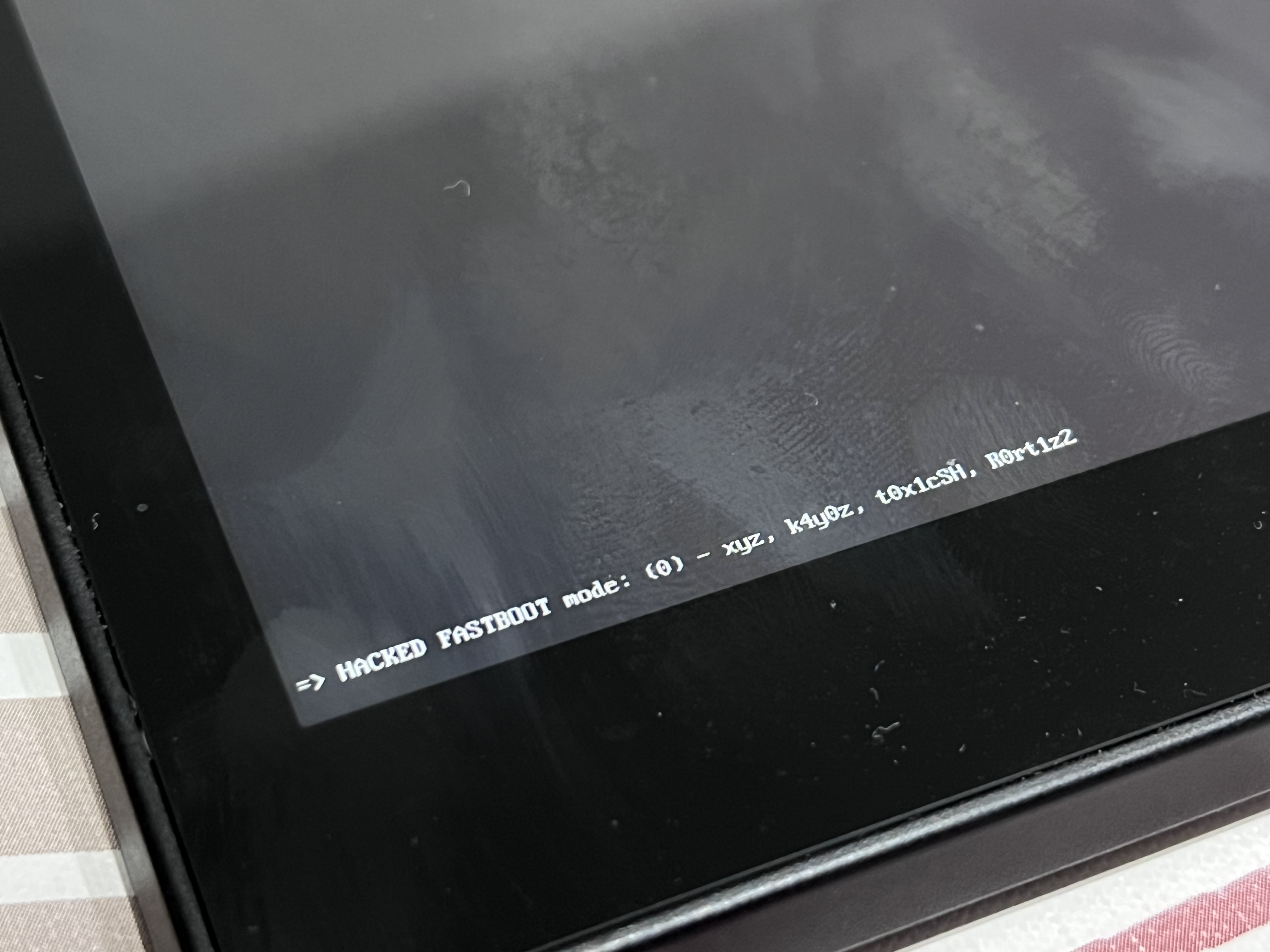
The functionality of the payload itself is the same as the one explained in my previous article. I just had to modify some parts to make it compatible with such an old device, such as the dev-read/write operations. You can check the full code here.
Demo of the PoC in action
Bonus: LineageOS 12.1
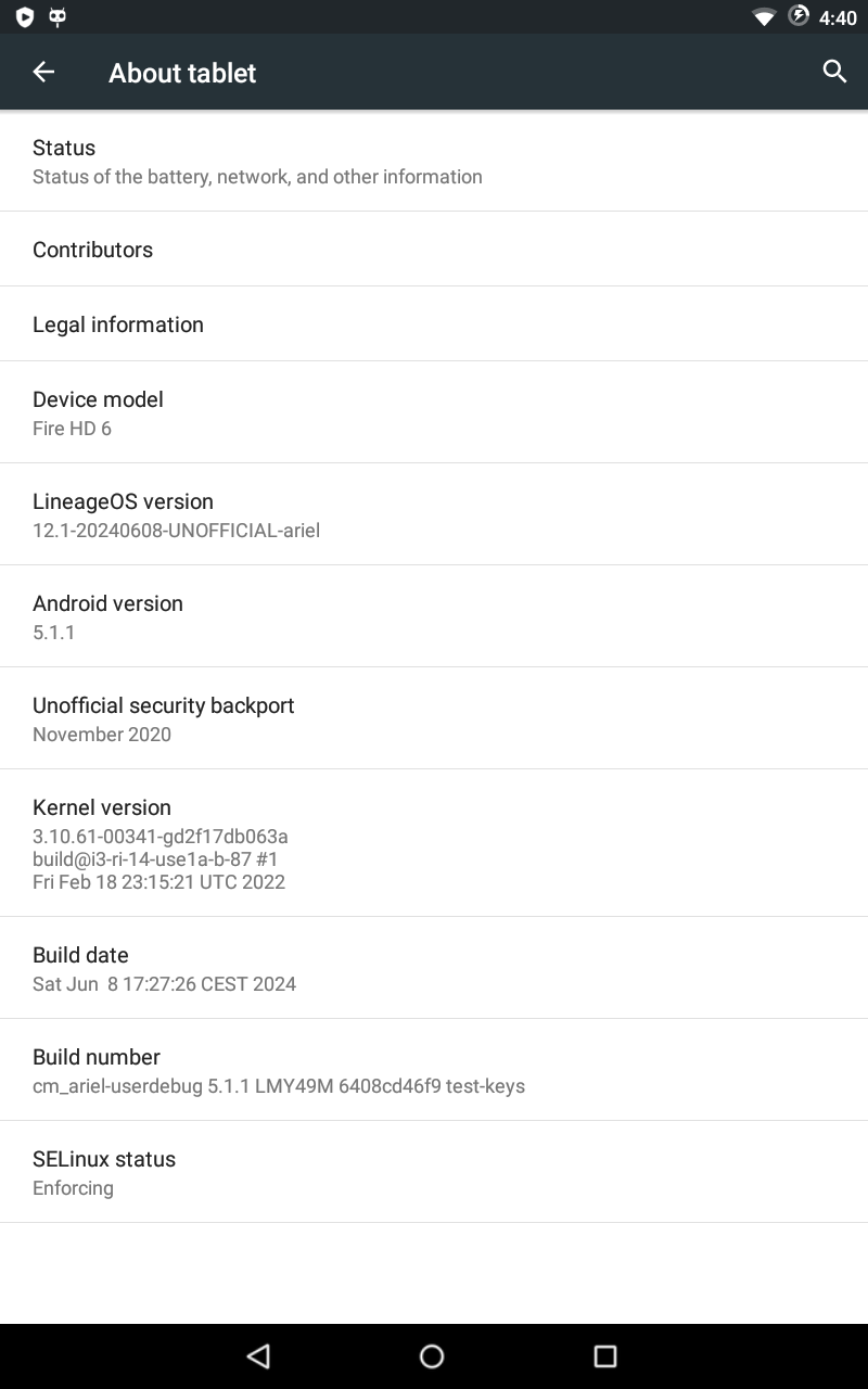
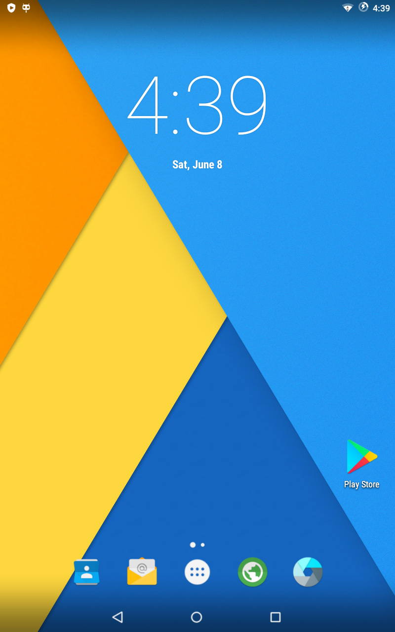
Considering how slow FireOS is, I decided it would be a great idea to have a smooth AOSP-based ROM. Since my motivation to build ROMs has been waning over the past few years, I didn't feel like bringing something newer than the latest stock version. Instead, I decided to build LineageOS 12.1 (formerly known as CyanogenMod 12.1) and make it as stable as possible.
After a few weeks of work, I managed to build a pretty solid ROM that runs 200 times faster than FireOS and is much more customizable. As of the time of writing, the only bug the ROM has is video recording, which crashes the Camera application. All the sources used to build both TWRP and LineageOS 12.1 can be found on this GitHub organization.
Conclusions
This was a fun journey, and I'm glad I managed to unlock the bootloader and build a custom ROM for the device. This process has helped me acquire a lot of knowledge about MediaTek devices and how they work at a low-level scope.
I'd like to thank k4y0z, t0x1cSH, and AntiEngineer for helping me with this project, both software and hardware-wise. I'd also like to thank zeroepoch and xyz for their amazing work on MediaTek devices. Nothing would have been possible without their contributions.
With this, I'm finishing this article. I hope you enjoyed reading it as much as I enjoyed writing it :)